SanDisk Develops 32nm NAND Flash Technology
![]() SanDisk and Toshiba have jointly announced the co-development of multi-level cell (MLC) NAND flash memory using 32-nanometer (nm) process technology to produce a 32-gigabit (Gb) 3-bits-per-cell (X3) memory chip. The breakthrough introduction is expected to quickly bring to market advanced technologies that will enable greater capacities and reduce manufacturing costs for products ranging from microSD memory cards to Solid State Drives (SSD).
SanDisk and Toshiba have jointly announced the co-development of multi-level cell (MLC) NAND flash memory using 32-nanometer (nm) process technology to produce a 32-gigabit (Gb) 3-bits-per-cell (X3) memory chip. The breakthrough introduction is expected to quickly bring to market advanced technologies that will enable greater capacities and reduce manufacturing costs for products ranging from microSD memory cards to Solid State Drives (SSD).
The 32Gb X3 on 32nm technology is the smallest NAND flash memory die reported so far, able to fit into the fingernail-sized microSD memory card format. Production is expected to begin in the second half of 2009.
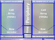
The 32nm 32Gb X3 is the highest density microSD memory die in the world, providing twice the capacity of a microSD chip on 43nm while still maintaining a similar die area. Advances in 32nm process technologies and in circuit design significantly contributed to a 113mm2 die-size while SanDisk's patented All-Bit-Line (ABL) architecture has been a key enabler to maintain a competitive X3 write performance.
 32GB microSD cards are likely to be the last capacity bump of the microSDHC line, which will be replaced by the next-generation SDXC (eXtended Capacity) memory card specification announced earlier this year. SDXC cards will be offered in capacities of 2 GB up to 2 TB with faster read/write speeds of up to 104 MB per second in 2009 with a road map to 300 MB per second.
"The development of our third-generation 3-bits-per-cell technology on 32nm within one and a half years after the introduction of the first generation of 3-bits-per-cell on 56nm shows the incredibly fast pace necessary to be a world-class producer in today's industry," said Sanjay Mehrotra, co-founder and president, SanDisk. "This allows us to offer higher capacities at compelling form factors while reducing manufacturing costs all helping to expand our various product lines. This new development highlights SanDisk's deep level of technical expertise and innovation that ultimately benefits consumers."
32nm is the most advanced flash memory technology node to date, requiring advanced solutions to manage the challenges of feature size scaling. 32nm technology combines several innovative technologies to reduce die area more aggressively than the trend-line of Moore's Law.
"32nm technology builds upon SanDisk's successful deployment of immersion lithography in 43nm to implement spacer process without incurring additional investment in capital-intensive lithography equipment," said Klaus Schuegraf, vice president, memory technology, SanDisk. "SanDisk brings its industry-leading 64-bit NAND string length to 32nm, while compensating for bit-to-bit interference effects with innovative programming algorithms and system design."
SanDisk and Toshiba today presented a joint paper on 32nm 32Gb X3 NAND flash memory at the 2009 International Solid State Circuits Conference (ISSCC), highlighting the technical advancements that made 32nm possible.
Leave a comment...
You must be registered and logged in to add comments.


Latest Comments
- I got one -Tuckermaclain
- RE: Don't we have this already? -Tuckermaclain
- RE: Palm brand will return in 2018, with devices built by TCL -richf
- RE: Palm brand will return in 2018, with devices built by TCL -dmitrygr
- Palm phone on HDblog -palmato
- Palm PVG100 -hgoldner
- RE: Like Deja Vu -PacManFoo
- Like Deja Vu -T_W